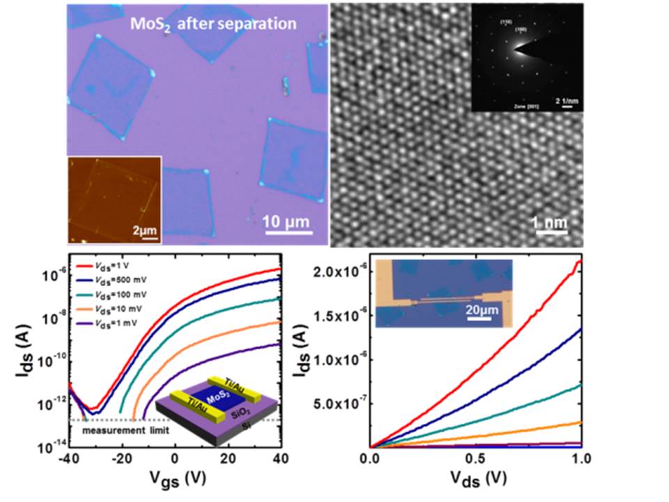
Semiconducting transition metal dichalcogenides (TMDCs), such as MoS2, have recently emerged as a family of 2D materials that are complementary to zero-bandgap graphene. The intrinsic, large bandgap (1.2-1.8 eV) of MoS2 atomic layers allows for their promising applications in nanoelectronics and optoelectronics. Liying Jiao and co-workers have developed a way to control the growth of crystalline MoS2 semiconductor by using MoO2 microcrystals as template. MoS2 atomic layers with regular shape and controlled number of layers of were obtained. Moreover, the obtained MoS2 flakes exhibited very high crystallinity with a crystal domain size of ~10 μm, comparable to exfoliated MoS2 flakes.The mobility of field effect transistors (FETs) made on these MoS2 flakes was also comparable with FETs based on mechanically exfoliated MoS2 flakes, further confirming the high quality of these MoS2 flakes. This approach will make high quality MoS2 flakes with desired shape and number of layers widely accessible for addressing many fundamental properties predicted for these materials and for exploring their potential applications. This work was published on J. Am. Chem. Soc.2013, 135, 5304 and was selected as Spotlights by J.Am.Chem.Soc. (2013, 135, 5475).